Understanding Solar Cells

Solar cell, photo effect, holes and photons?
Explanations of the principles of a solar cell are normally hard to follow by non-experts.
However, this is also possible in a clear and understandable way as you can see at the following book excerpt.
Understanding the relatively complicated way that solar cells work requires immersion into the most extreme depths of high physics. The small applied model shown in Figure 1 explains roughly the principle involved. There are two horizontal levels. The second level is located a bit higher than the first one. The first level has a large number of small hollows filled to the top with water. The water here cannot move by itself. Now someone starts to throw small rubber balls at the first level. If a ball hits a hole, the water splashes upwards and ends up on the second level. Here there are no hollows to contain the water. The second level is therefore inclined so that the water runs off and reaches the draining groove on its own. This groove is connected to the second level through a pipe and as the water flows through, it drives a small waterwheel with a dynamo. When the water reaches the lower level, it fills up the hollows again. The cycle can start all over again with new rubber balls.

Figure 1: Model illustrating the processes of a solar cell
However, we want to use solar cells not to produce a water cycle but to generate electric current to run electrical appliances. Electric current is created from the flow of negative-charge carriers, called electrons. These are the same as the water in our simple model. The solar cell needs a material in which two levels can be found: one level in which the electrons are firmly affixed like the water collecting in the hollows, and a second level where the electrons are able to move freely. Semiconductor materials normally have precisely these properties. Tiny particles of light, called photons in physics, correspond to the rubber balls and are able to raise the electrons to the second level.
The tilt in our simple model is important because it enables the cycle to function perfectly. Otherwise the water will not collect on its own in the rain gutter. With semiconductors the second level must also have an incline that enables the electrons to gather on one side. In contrast to our simple model, it is not gravity that is used to collect the electrons but instead an electric field, which pulls the negatively charged electrons to one side. In order to produce this field, a semiconductor must be ‘doped’. One side of the semiconductor is deliberately contaminated with an element like boron and the other side with a different element like phosphorus. As boron and phosphorus also have a varying number of electrons, they produce the necessary incline. The crossing area is called a space-charge region. An electric field is created here, which pulls the electrons to one side. There external contacts collect them and they flow back to the first level through an external electric circuit. In the process they produce electrical energy.
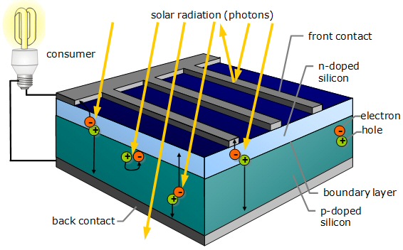
Figure 2 shows the principal structure of a silicon solar cell. In technical jargon the different doped sides of the silicon wafer are called n-doped and p-doped silicon, respectively. Between the two areas is a barrier layer with the space-charge region. Light in the form of photons separates negatively charged particles (electrons) and positively charged particles (holes) and ensures that the electrons are able to move about freely at the second level. In contrast to the simple model shown, the holes also move. The electrons and holes are separated by the space-charge region. Thin front contacts collect the electrons on the front side of the cell.
However, not every light particle ensures that an electron is separated from the hole. If the energy of the photon is too low, the electron will fall back into the hole. On the other hand, if the energy of the photon is too high, only part of it is used to separate the electron from the hole. Some photons also move through the solar cell unused; others are reflected by the front contacts.
